- 您现在的位置:买卖IC网 > Sheet目录3753 > ATMEGA169P-16MCHR (Atmel)MCU AVR 16KB FLASH 16MHZ 64-VQFN
PIC16F946
DS41265A-page 236
Preliminary
2005 Microchip Technology Inc.
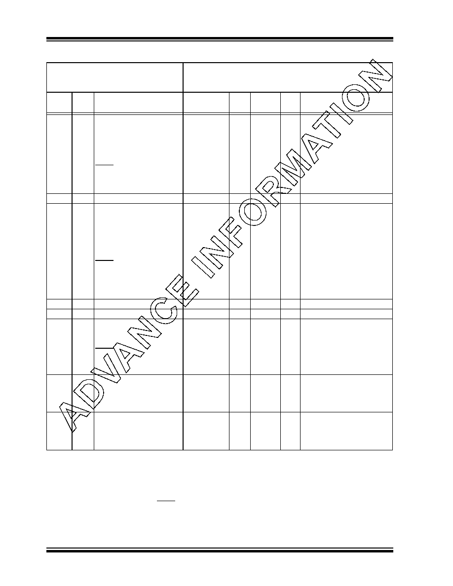
19.4
DC Characteristics: PIC16F946-I (Industrial), PIC16F946-E (Extended)
DC CHARACTERISTICS
Standard Operating Conditions (unless otherwise stated)
Operating temperature
-40°C
≤ TA ≤ +85°C for industrial
-40°C
≤ TA ≤ +125°C for extended
Param
No.
Sym
Characteristic
Min
Typ
Max
Units
Conditions
VIL
Input Low Voltage
I/O port:
D030
with TTL buffer
VSS
—0.8
V
4.5V
≤ VDD ≤ 5.5V
D030A
VSS
—0.15 VDD
V
Otherwise
D031
with Schmitt Trigger buffer
VSS
—
0.2 VDD
V
Entire range
D032
MCLR, OSC1 (RC mode)
VSS
—
0.2 VDD
V
D033
OSC1 (XT and LP modes)(1)
VSS
—0.3
V
D033A
OSC1 (HS mode)(1)
VSS
—
0.3 VDD
V
D034
I2C mode
VSS
—0.3VDD
VEntire VDD Range
VIH
Input High Voltage
I/O port:
—
D040
D040A
with TTL buffer
2.0
(0.25 VDD +
0.8)
—
VDD
V
4.5V
≤ VDD ≤ 5.5V
Otherwise
D041
with Schmitt Trigger buffer
0.8 VDD
—VDD
V
Entire range
D042
MCLR
0.8 VDD
—VDD
V
D043
OSC1 (XT and LP modes)
1.6
—
VDD
V
(Note 1)
D043A
OSC1 (HS mode)
0.7 VDD
—VDD
V
(Note 1)
D043B
OSC1 (RC mode)
0.9 VDD
—VDD
V
D044
I2C mode
0.7VDD
—VDD
VEntire VDD Range
D070
IPUR
PORTB Weak Pull-up Current
50*
250
400*
μAVDD = 5.0V, VPIN = VSS
IIL
Input Leakage Current(2)
D060
I/O port
—
± 0.1
± 1
μAVSS ≤ VPIN ≤ VDD,
Pin at high-impedance
D061
MCLR(3)
—
± 0.1
± 5
μAVSS ≤ VPIN ≤ VDD
D063
OSC1
—
± 0.1
± 5
μAVSS ≤ VPIN ≤ VDD, XT, HS and
LP OSC configuration
VOL
Output Low Voltage
D080
I/O port
—
0.6
V
IOL = 8.5 mA, VDD = 4.5V (Ind.)
D083
OSC2/CLKO (RC mode)
—
0.6
V
IOL = 1.6 mA, VDD = 4.5V (Ind.)
IOL = 1.2 mA, VDD = 4.5V (Ext.)
VOH
Output High Voltage
D090
I/O port
VDD – 0.7
—
V
IOH = -3.0 mA, VDD = 4.5V (Ind.)
D092
OSC2/CLKO (RC mode)
VDD – 0.7
—
V
IOH = -1.3 mA, VDD = 4.5V (Ind.)
IOH = -1.0 mA, VDD = 4.5V (Ext.)
*
These parameters are characterized but not tested.
Data in ‘Typ’ column is at 5.0V, 25
°C unless otherwise stated. These parameters are for design guidance only
and are not tested.
Note 1:
In RC oscillator configuration, the OSC1/CLKI pin is a Schmitt Trigger input. It is not recommended to use an
external clock in RC mode.
2:
Negative current is defined as current sourced by the pin.
3:
The leakage current on the MCLR pin is strongly dependent on the applied voltage level. The specified levels
represent normal operating conditions. Higher leakage current may be measured at different input voltages.
发布紧急采购,3分钟左右您将得到回复。
相关PDF资料
2-1546217-0
TERM BLK RCPT 20POS SIDE 5.08MM
1-1546217-9
TERM BLK RCPT 19POS SIDE 5.08MM
1-1546217-8
TERM BLK RCPT 18POS SIDE 5.08MM
1-1546217-7
TERM BLK RCPT 17POS SIDE 5.08MM
1-1546217-6
TERM BLK RCPT 16POS SIDE 5.08MM
1-1546217-5
TERM BLK RCPT 15POS SIDE 5.08MM
1-1546217-4
TERM BLK RCPT 14POS SIDE 5.08MM
1-1546217-3
TERM BLK RCPT 13POS SIDE 5.08MM
相关代理商/技术参数
ATMEGA169P-16MCU
功能描述:8位微控制器 -MCU AVR 16KB, 512B EE 16MHz 1KB SRAM, 5V
RoHS:否 制造商:Silicon Labs 核心:8051 处理器系列:C8051F39x 数据总线宽度:8 bit 最大时钟频率:50 MHz 程序存储器大小:16 KB 数据 RAM 大小:1 KB 片上 ADC:Yes 工作电源电压:1.8 V to 3.6 V 工作温度范围:- 40 C to + 105 C 封装 / 箱体:QFN-20 安装风格:SMD/SMT
ATMEGA169P-16MU
功能描述:8位微控制器 -MCU AVR 16K FLASH 512B EE 1K SRAM LCD ADC RoHS:否 制造商:Silicon Labs 核心:8051 处理器系列:C8051F39x 数据总线宽度:8 bit 最大时钟频率:50 MHz 程序存储器大小:16 KB 数据 RAM 大小:1 KB 片上 ADC:Yes 工作电源电压:1.8 V to 3.6 V 工作温度范围:- 40 C to + 105 C 封装 / 箱体:QFN-20 安装风格:SMD/SMT
ATMEGA169P-16MU SL383
制造商:Atmel Corporation 功能描述:MCU 8BIT ATMEGA RISC 16KB FLASH 3.3V/5V 64PIN MLF - Tape and Reel
ATMEGA169P-16MUR
功能描述:8位微控制器 -MCU AVR LCD 16KB FLSH EE 512B 1KB SRAM-16MHZ RoHS:否 制造商:Silicon Labs 核心:8051 处理器系列:C8051F39x 数据总线宽度:8 bit 最大时钟频率:50 MHz 程序存储器大小:16 KB 数据 RAM 大小:1 KB 片上 ADC:Yes 工作电源电压:1.8 V to 3.6 V 工作温度范围:- 40 C to + 105 C 封装 / 箱体:QFN-20 安装风格:SMD/SMT
ATMEGA169P-8AU
制造商:ATMEL 制造商全称:ATMEL Corporation 功能描述:Microcontroller with 16K Bytes In-System Programmable Flash
ATMEGA169P-8MU
制造商:ATMEL 制造商全称:ATMEL Corporation 功能描述:Microcontroller with 16K Bytes In-System Programmable Flash
ATMEGA169PA
制造商:ATMEL 制造商全称:ATMEL Corporation 功能描述:8-bit Microcontroller with 16K Bytes In-System Programmable Flash
ATMEGA169PA_1
制造商:ATMEL 制造商全称:ATMEL Corporation 功能描述:High Endurance Non-volatile Memory segments